

 Home
Home


Silicon Wafers Type P/B Prime Grade Sio Oxide Silicon Wafers Slices Substrates
Overview 25PCS/Lot Solar Silicon Wafers 3 Inches Type P/B Prime Grade Sio Wafers Oxide Silicon Wafers Slices Substrates
Send your inquiryDESCRIPTION
Basic Info
| Model NO. | FW-CRYSTAL |
| Growth Method | CZ and Fz |
| Orientation | 111 or 100 |
| Resistivity | 0.0005 to 150 |
| Surface | Double Side Polished or Single Side Polished |
| Dopant | N Type and P Type |
| Particles | <30 at 0.3um |
| Bow | < 30 Um |
| Ttv | <15 Um |
| Transport Package | Box |
| Specification | costomized |
| Trademark | FW |
| Origin | China |
| Production Capacity | 100, 000PCS/Month |
Product Description
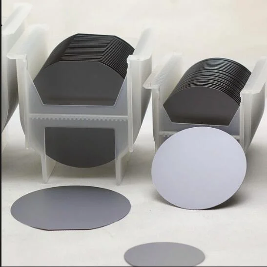
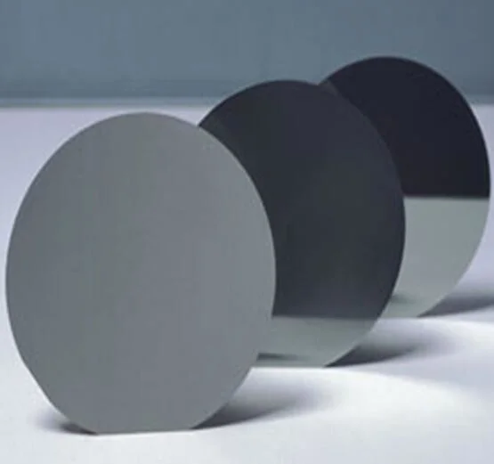
25PCS/Lot Solar Silicon Wafers 3 Inches Type P/B Prime Grade Sio Wafers Oxide Silicon Wafers Slices Substrates
1. what is silicon wafers and it's application:
A silicon wafer is a material essential for manufacturing semiconductors, which are found in all kinds of electronic devices that enrich our lives.
Silicon wafer is the most common material and widely used for a varity of high-tech industries, including integrated circuits, detector or sensor device, MEMS fabrication, opto-electronic components, and solar cells.
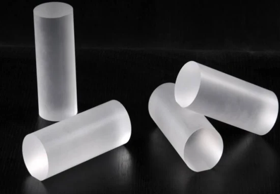
Silicon wafer is a very thin round disk cut from high-purity silicon. A round silicon ingot is sliced to thicknesses of approximately 1mm. The surfaces of the resulting disk are polished carefully, then it is cleaned, resulting in the completed wafer. Silicon wafers are made from high-purity silicon, and are the material of semiconductor devices. These wafers can also be fabricated with a SEMI notch or one or two SEMI flats.
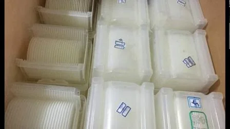
Detailed Photos
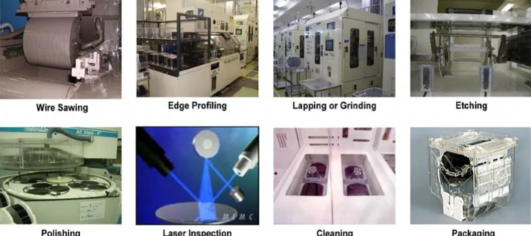
Manufacturing a Silicon Wafer
Growing a silicon ingot can take anywhere from one week to one month, depending on many factors, including size, quality and the specification. More than 75% of all single crystal silicon wafers grow via the Czochralski (CZ) method.
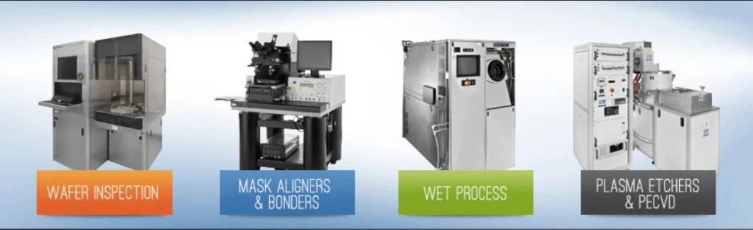
Equipment we use
| Grow method | CZ or FZ |
| Diameter | 1 to 8 inch |
| Finish | As cut, lapped, etched, SSP, DSP |
| Orientation | (100) (111) (110) |
| Type | N or P |
| Resistivity | CZ: From 0.0005 to 150 Ωcm FZ: Up to 10 kΩcm |
Q: What's the way of shipping and cost?
A:(1) We accept DHL, Fedex, TNT, UPS, EMS etc.
(2) If you have your own express account, it's great.If not,we could help you ship them.
Q: How to pay?
A: T/T, Paypal, etc
Q: What's your MOQ?
A: (1) For inventory, the MOQ is 5pcs.
(2) For customized products, the MOQ is 10pcs-25pcs.
Q: What's the delivery time?
A: (1) For the standard products
For inventory: the delivery is 5 workdays after you place the order.
For customized products: the delivery is 2 or 3 weeks after you place the order.
(2) For the special-shaped products, the delivery is 4 or 6 workweeks after you place the order.
Q: Do you have standard products?
A: Our standard products in stock.
Q: Can I customize the products based on my need?
A: Yes, we can customize the material, specifications and optical coating for your optical components based on your needs.
Related Products
-
![Bbo Nonlinear Crystal Surface Quality 10-5 S-D with Extremely Low Absorption Coefficient]()
Bbo Nonlinear Crystal Surface Quality 10-5 S-D with Extremely Low Absorption Coefficient
-
![Hot New Product Toxina Botulinica Liztox Re N Tox Novatox 100 Unit 200 Unit Hyaluronic Acid Ha Filler Neuramis Revolax Bonetta Best Slimming Products Lipo Lab]()
Hot New Product Toxina Botulinica Liztox Re N Tox Novatox 100 Unit 200 Unit Hyaluronic Acid Ha Filler Neuramis Revolax Bonetta Best Slimming Products Lipo Lab
-
![Er: Yb: Glass Crystal Erbium and Ytterbium Co-Doped Phosphate Glass Laser]()
Er: Yb: Glass Crystal Erbium and Ytterbium Co-Doped Phosphate Glass Laser
-
![1500/1800rpm Speed and Cheap Diesel Generator Rated Current Power Generator]()
1500/1800rpm Speed and Cheap Diesel Generator Rated Current Power Generator


