

 Home
Home
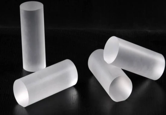


Supply Single Crystal Silicon Wafer Si Substrate Type N/P for Infrared Optical Materials
Customized Single Crystal Silicon Wafer Si Substrate Type N/P Optional Silicon Wafer 1. what is Oxide silicon wafers and
Send your inquiryDESCRIPTION
Basic Info
| Model NO. | FW-LN |
| Manufacturing Technology | Optoelectronic Semiconductor |
| Material | Compound Semiconductor |
| Type | Intrinsic Semiconductor |
| Package | SMD |
| Signal Processing | Analog Digital Composite and Function |
| Application | LED |
| Model | 1324 |
| Batch Number | Polished |
| Brand | Finewen |
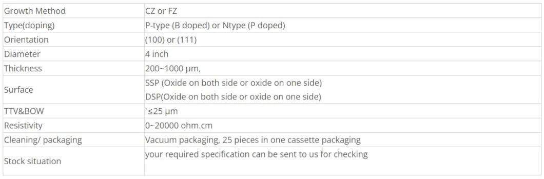
| Growth Method | CZ and Fz |
| Orientation | 111 or 100 |
| Resistivity | 0.0005 to 150 |
| Surface | Double Side Polished or Single Side Polished |
| Dopant | N Type and P Type |
| Particles | <30 at 0.3um |
| Bow | < 30 Um |
| Ttv | <15 Um |
| Transport Package | Box |
| Specification | customized size |
| Trademark | FW-Wafers |
| Origin | Jiaozuo Henan |
| Production Capacity | 100, 000PCS/Month |
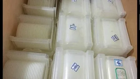
Product Description
Customized Single Crystal Silicon Wafer Si Substrate Type N/P Optional Silicon Wafer
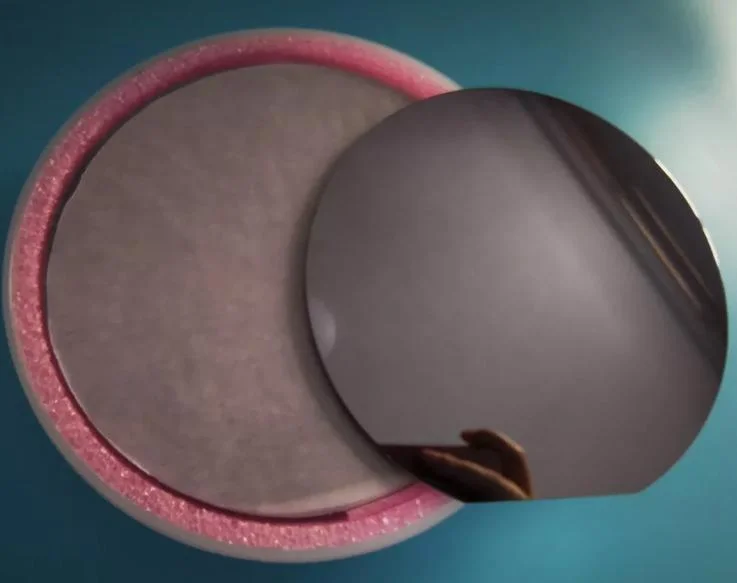
1. what is Oxide silicon wafers and it's application:
The silicon thermal dioxide wafer refers to the thermal growth of a uniform dielectric film on the surface of the silicon wafer, which is used as an insulation or mask material. The oxidation process includes high temperature dry oxygen oxidation and high temperature wet oxygen oxidation.
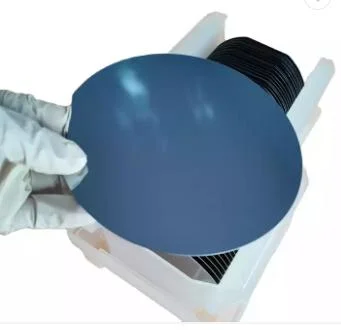
2.Product discriptio
Product Name | CZ and FZ Polished silicon Wafer |
Material | Silicon |
Diameter | 150mm |
Surface finish | SSP |
Orientation | NO Request |
Grade | None |
Type | None |
Resistivity | None |
Thickness | 2500um |
Growing a silicon ingot can take anywhere from one week to one month, depending on many factors, including size, quality and the specification. More than 75% of all single crystal silicon wafers grow via the Czochralski (CZ) method.
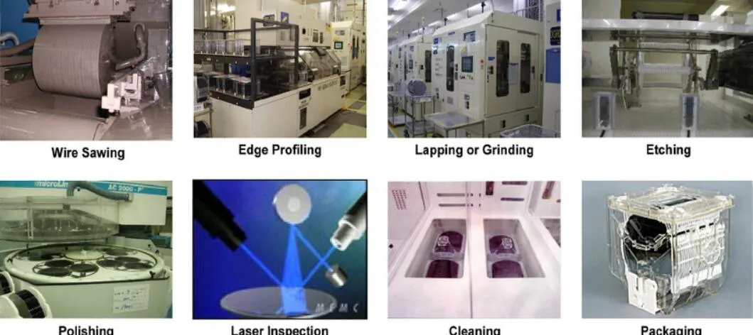
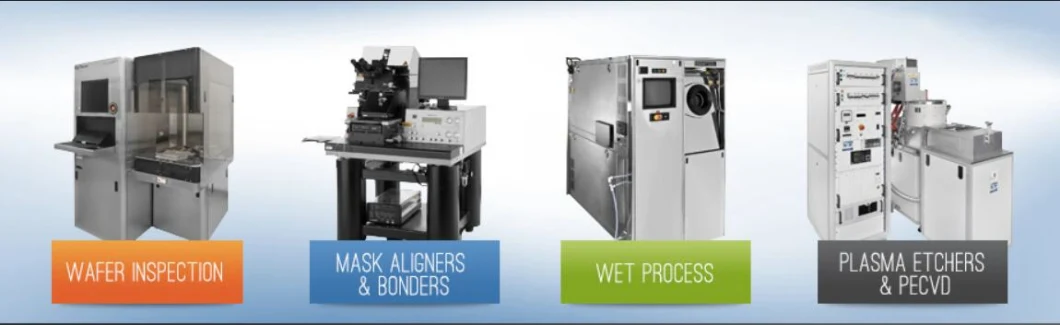
4.Equipment we use
6.FAQ:
Q: What's the way of shipping and cost?
A:(1) We accept DHL, Fedex, TNT, UPS, EMS etc.
(2) If you have your own express account, it's great.If not,we could help you ship them.
Q: How to pay?
A: T/T, Paypal, etc
Q: What's your MOQ?
A: (1) For inventory, the MOQ is 5pcs.
(2) For customized products, the MOQ is 10pcs-25pcs.
Q: What's the delivery time?
A: (1) For the standard products
For inventory: the delivery is 5 workdays after you place the order.
For customized products: the delivery is 2 or 3 weeks after you place the order.
(2) For the special-shaped products, the delivery is 4 or 6 workweeks after you place the order.
Q: Do you have standard products?
A: Our standard products in stock.
Q: Can I customize the products based on my need?
A: Yes, we can customize the material, specifications and optical coating for your optical components based on your needs.
Related Products
-
![Custom Optical Glass Znse Crystal Cylindricall Meniscus Lens for Laser Machine]()
Custom Optical Glass Znse Crystal Cylindricall Meniscus Lens for Laser Machine
-
![15*15mm Factory Price CVD Single Crystal Diamond Plate CVD Diamond Substrate]()
15*15mm Factory Price CVD Single Crystal Diamond Plate CVD Diamond Substrate
-
![Piezoceramics Piezoelectric Ring Pzt Piezo Ceramics Crystals for Ultrasonic Cleaner]()
Piezoceramics Piezoelectric Ring Pzt Piezo Ceramics Crystals for Ultrasonic Cleaner
-
![Polished Yv04 Crystal for Diode Laser-Pumped Solid-State Lasers]()
Polished Yv04 Crystal for Diode Laser-Pumped Solid-State Lasers


