

 Home
Home
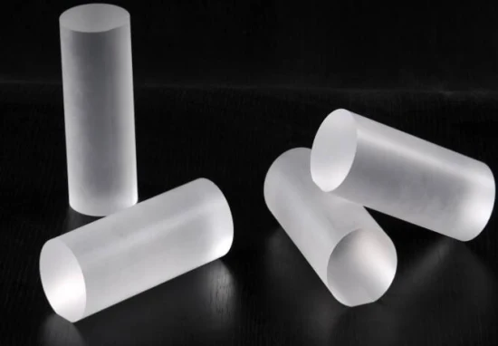


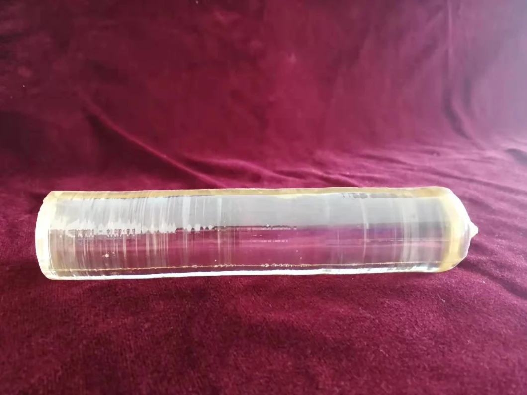
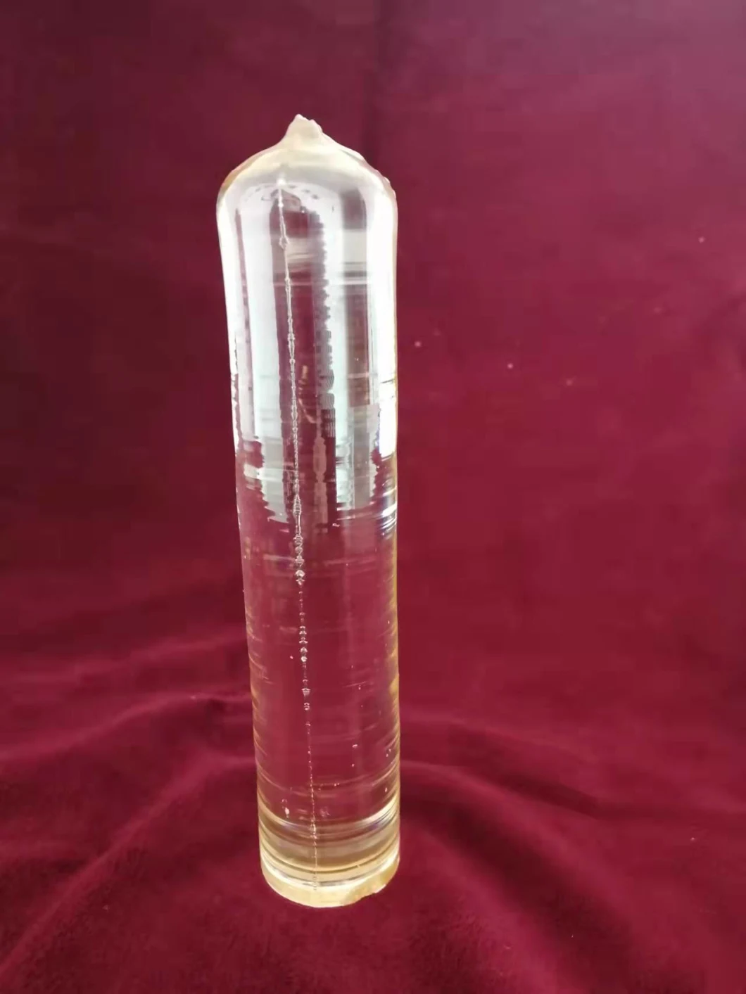
Lithium Niobate (LiNbO3) Crystal Substrate Wafer
Overview Product Description Compared with congruent lithium niobate crystal (abbreviated: herculean task), SLNS due to
Send your inquiryDESCRIPTION
Basic Info
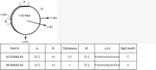
| Model NO. | FW-LN |
| Dopping | Fe,Mg,MGO |
| Transport Package | Single Piece or 25 PCS |
| Specification | 2-6 inch |
| Trademark | FineWin |
| Origin | China |
Product Description
Compared with congruent lithium niobate crystal (abbreviated: herculean task), SLNS due to the increase of lithium content detected (close to 50 mol 1%),Drastically reduces the crystals in Li space (VLi), niobium (NbLi) intrinsic defects, such as physical properties and optical properties of crystals are increased sharply, measurement than lithium niobate crystal as holographic storage, electro-optic switch, optical information processing, optical waveguide and dielectric superlattices in many fields such as the most potential of crystal materials.
Product Parameters| crystal structure | trigonal system |
| space groups | C36(R3C) |
| melting point | 1260ºC |
| Moh's hardness | ~4.8 |
| density | 4.46g/cm3 |
| coefficient of thermal expansion | 16.7(∥a) 2(∥a) |
| Optical transparency range | 370~5000nm |
| refractive index | (633nm)n0=2.286 ne=2.200 |
Currently available with 2-2.5 inches (mixed magnesium) than near stoichiometric lithium niobate crystal and chip products.
Application
An important material for optical waveguides, mobile phones, piezoelectric sensors, optical modulators and a variety of other linear and nonlinear optical applications.
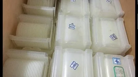
Packaging
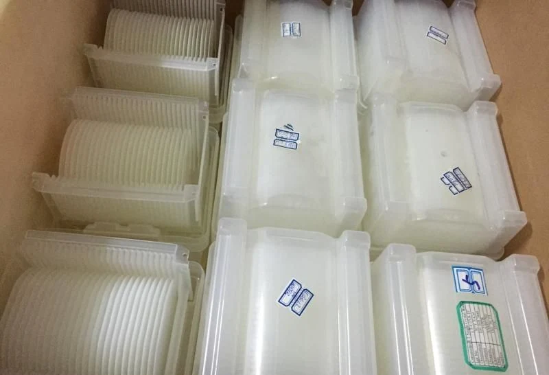
Detailed Photos
Related Products


